
Talk about high-end switches again
Release time:
2023-06-12
In control systems, it is common to encounter the need to switch on/off a specific payload
In control systems, it is common to encounter the need to switch on/off a specific payload or multiple payloads at a certain moment.This requires adding switches at the lower end of the power bus. There are two common modes of switches, as shown in the figure below:
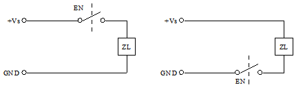
High-end switch Low-end switch
Both types have their uses. High-end switches are mainly used in high/medium voltage applications;;Low-end switches are mainly used in5V/3.3V application scenarios. The following mainly analyzes high-end switches.
In principle, high-end switches are most conveniently implemented using relays, and the contact resistance of relays is very small (generally a fewmilliohms, depending on the size of the contact area). However, modern electronic systems generally try to avoid using relays. The reason is that at the moment of relay engagement/disengagement (when the distance between two contacts is in Depending on the size of the contact area. However, in modern electronic systems, relays are generally avoided as much as possible. The reason is that it is easy to occur at the moment when the relay is engaged/disconnected (when the distance between the two contacts is in um level)"arc" (especially in medium/high voltage situations), which affects system lifespan.
Therefore, modern electronic systems generally useMOS-FETs as switching elements, also known as "contactless switches." Compared to relays, they have larger conduction losses (because MOSFETs cannot achieve such low conduction resistance), but their advantages include no mechanical action and thus longer lifespan. Additionally, they can switch quickly (which is crucial for some loads). Using MOSFETs as high-end switches can be divided into two cases:
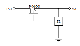
P-MOS:(easier to implement). However, due to the low mobility of "holes," they are generally only suitable for medium voltage (10V~100V) and medium power (≤10A) applications. The mobility of "holes" is low, so they are generally only suitable for medium voltage (10V-100V) and medium power (≤ 10A) applications.
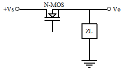
N-MOS:(N-MOS: requires "floating gate" drive, difficult to implement. However, due to the high mobility of "electrons," they are suitable for high voltage (≥200V) and high power (≥50A) applications. The 'floating gate' drive is difficult to implement. However, due to the high mobility of "electrons", it is suitable for applications with high voltage (≥ 200V) and high power (≥ 50A).
These two types of switches can control the speed of turning on/off arbitrarily to meet different load requirements. In the figure above, /Close the speed to adapt to different ZL load requirements. Δ V in the figure represents the conduction voltage drop of the MOS transistor.

Quick switch: only conduction loss. Suitable for high-frequency applications.

Slow switch: In addition to static losses, there are also switch losses, which are power losses caused by MOS transistor gate source charging/discharging. Suitable for situations where switches are not frequently used.
Due to conduction and switching losses, adjustments should be made to the control strategy of MOS transistors and corresponding heat dissipation should be applied based on system control requirements and load conditions in applications.
So, what are the components of a completed high-end switch? Let's take P-MOS transistor as an example to illustrate. (See the diagram below)
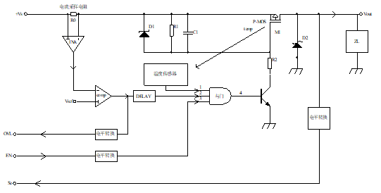
From the above diagram, it can be seen that a typical medium voltage and medium power high-end switch consists of a switching transistor (M1), current sampling (R0), high common mode voltage instrumentation amplifier (INA), comparator (COMP), delay, AND logic gate, level conversion, and RC network for controlling on/off rate. OVL "is an overcurrent indicator," SO "is an output indicator, and" EN "is an on/off control signal. This combination is more suitable for aviation 28V power systems. Because the composition is not complex, the volume is small, and it is easy to implement.
Several core points of this system need to be specifically explained as follows:
power waste. It mainly depends on the conduction resistance RON of M1 (excluding switching losses) and the size of the current sampling resistance RO. Generally, RON and RO are chosen to be as small as possible.
Switching speed control. By adjusting R1, R2, and C1, it depends on the characteristics of the load. If the load exhibits pure resistance characteristics, it is suitable for fast switching control to reduce the dynamic power consumption of M1. If the load exhibits capacitive for resistive loads, only a slow switch control strategy can be adopted. This is because the voltage across the capacitor cannot change abruptly, and the current through the inductor cannot change abruptly. If the switching rate is too fast, it may easily cause false triggering of overcurrent detection and also pollute the power supply system.
Overcurrent hiccup state (hiccup), achieved by adjusting the delay of the comparison output and controlling M1rising/falling time together. The hiccup state is a function that should be present in all power supply systems. It meets the characteristics shown in the figure below.

That is to say, when the upstream machine sends outthe EN signal, the high-side switch should be in a normal power supply state. However, if load ZLexperiences overload (such as a short circuit), then the current sensing resistorR0detects this overcurrent, leading to local controlM1cutoff.M1After cutoff, the overcurrent state disappears and normal power supply resumes. However, since the overcurrent state still exists, the system attempts to shut down again.M1This cycle will produce waveforms similar to those shown in the figure above, commonly referred to as"hiccup state."
Its importance lies in two aspects: first, it protects components from burning out by intermittently turning off switch tubes locally.M1Second, after detecting an overcurrent indication signal from the upper computer labeled "OVL" for a certain number of hiccups, it issues an EN command for remote shutdown of M.-level conversion is mainly designed for compatibility with signals from upper central control computers. Sometimes due to grounding issues between central control computers and1。
+V-S power systems not sharing ground, isolation needs to be added.'s role is to protect's gate-source from breakdown.'s role is to maintain load continuity when disconnected....The above discusses implementation methods for high-end switches with medium voltage and medium power.
...Next, I will briefly introduce an implementation strategy for high-voltage high-power high-end switches.1...The primary consideration in designing high-voltage high-power high-end switches is to reduce power consumption. Therefore, the previously mentionedM1"Shunt" type current sensing cannot be used anymore. Additionally, due to P-MOS transistors' mobility issues and manufacturing process factors, achieving voltage ratings above...Next, I will briefly introduce an implementation strategy for high-voltage high-power high-end switches.2(see block diagram below)M1...As a complete design of a high-end switch besides considering basic components,
...the characteristics of loads (i.e., ZL in above figure).
...capacitance C,
...while inductance's continuous flow effect causes negative voltage pulses during cutoff....Finally,...environmental stress should also be considered” Type current sampling cannot be used. In addition, due to the mobility issue and manufacturing process factors of P-MOS transistors, it is difficult to achieve a withstand voltage of ≥ 200V and a small on resistance Ron, and it must be replaced with N-MOS transistors to achieve this; Secondly, considering that crosstalk on the power ground (PGND) can affect/burn out the upper central control computer, OVL, EN, and SO signals must be isolated; Another issue is heat dissipation. Sometimes air cooling is no longer reliable, and oil/water cooling must be used to dissipate heat from M1. (See the diagram below)
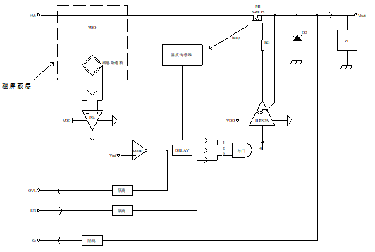
From the above figure, it can be seen that N-MOS transistor is used as the switching element, magnetic Wheatstone bridge is used as the current sampling, HJ393A is used to drive N-MOS, and a temperature sensor is added to measure the junction temperature of N-MOS. The control power supply VDD needs to be introduced. This combination is beneficial for reducing power consumption (without the aforementioned RO), and can achieve floating gate driving for N-MOS as well as over temperature protection.
As a comprehensive high-end switch design, in addition to considering the basic composition, it is also necessary to consider the characteristics of the load (i.e. ZL in the above figure). Pure resistive loads do not exist. Generally, loads are a combination of resistor R, capacitor C, and inductor L. The energy storage function of capacitors can cause a current surge at the moment when switch transistor M1 is turned on, and the freewheeling effect of inductors can cause M1 to withstand negative voltage pulses when it is turned off. These factors will have a negative impact on the long-term reliable operation of power transistor M1.
Finally, as a high-end switch for applications in harsh environments. Environmental stress should also be considered (For example, temperatureStress,Impact/Vibrational stress、Electromagnetic environmental stressand so on)Adaptability.
Key words:
control ,encounter
Previous Page
recommend News
Essential Insights on Power Amplifiers for Motor Control Applications
Power amplifiers for motor control are vital components in various electronic systems, serving as the bridge between low-level control signals and the high-power requirements of motors. These amplifiers are designed to deliver significant power gains, enabling precise control over motor speed, torque, and direction. Understanding their functionality and selection criteria can greatly enhance the p
2026-06-30
Common Mistakes to Avoid When Using Rail-to-Rail Amplifiers
Common Mistakes to Avoid When Using Rail-to-Rail Amplifiers Rail-to-rail amplifiers are powerful tools in the electronics industry, enabling designers to maximize the output signal range of their circuits. While these amplifiers can significantly enhance performance, many users make common mistakes that can lead to suboptimal results. In this article, we will delve into these pitfalls, providing v
2026-06-29
Unlocking the Potential of Rail-to-Rail Amplifiers in Sensor Interfaces
Rail-to-rail amplifiers are pivotal components in modern electronic systems, particularly in sensor interfaces where precision and efficiency are paramount. These amplifiers are designed to operate over the full voltage range from the negative rail to the positive rail, enabling them to effectively utilize the entire supply voltage. This characteristic is especially beneficial in applications requ
2026-06-28
Understanding the Advanced Technology Behind Low Voltage Rail-to-Rail Operational Amplifiers
Understanding the Advanced Technology Behind Low Voltage Rail-to-Rail Operational Amplifiers Table of Contents 1. Introduction to Rail-to-Rail Operational Amplifiers 2. What is a Rail-to-Rail Operational Amplifier? 3. The Importance of Low Voltage in Modern Electronics 4. Key Design Principles of Rail-to-Rail Op-Amps 5. Applications of Rail-to-Rail Operational Amplifiers 6
2026-06-27
Understanding Precision Amplifiers in Data Acquisition Systems
Precision amplifiers are fundamental elements in data acquisition systems, particularly in applications requiring high accuracy and low noise levels. These amplifiers are engineered to amplify small voltage signals while maintaining fidelity and precision, which is critical in various electronic processing tasks. A data acquisition system (DAS) typically consists of sensors, signal conditioning c
2026-06-26