
Hangjing has announced the upgrade and optimization of domestically produced products.
Release time:
2023-08-12
In the spirit of being responsible to customers and continuous improvementction.
In the spirit of being responsible to customers and continuous improvement, for a long timeHangjing Company has been developing and producing new products based on market or customer needs, as well as researching domestic alternatives to imported integrated circuits, while also continuously upgrading and improving existing mass-produced standardized products.upgrading andimproving,to make circuit electrical parameters better, applications more extensive, and enhance system performance,to meet customer needs to the greatest extent.
Recently, our company has completed the domestic replacement of imported operational amplifiersOP07Aand instrumentation amplifiersAD620.The work on the improvement and optimization of the productsdomestic replacement的产品HJOP07与HJG620. The technical staff conducted multiple tests on the devices,, completing and verifying that their electrical parameters have been overall optimized based on the original foundation, reaching the electrical performance indicators of imported devices, with some parameters even better than those of imported devices.
HJOP07. Product improvement
Is a low-noise, non-chopping zero-stabilized bipolar operational amplifier.HJOP07. It features low input bias current, high open-loop gain, wide input voltage range, high common-mode rejection ratio, high input impedance, etc. It is mainly used in high-gain measurement equipment and weak signal processing for amplifying sensors. It can provide high precision for inverter circuit configurations and can be widely applied in miniaturized high-performance instruments in defense, military applications, oil exploration, and industrial fields.
We, through fine-tuning optimization during the wafer production stage Fine tuning and optimization are carried out during the production phase to ensure that the final packaged product HJOP07 can achieve very low input offset voltage, and no additional zeroing measures are required during use.
1. Packaging form
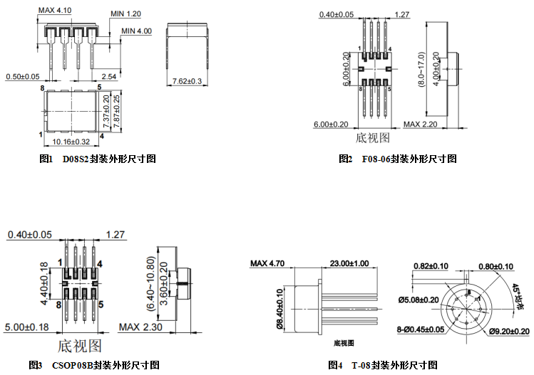
The packaging adopts D08S2 ceramic dual in-line package, CSOP08B surface mount 8-wire micro package, T-08 metal round 8-wire package, and F08-06 ceramic flat package. The specific packaging size diagram is shown in the appendix.
2. Lead out function
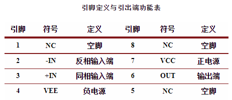
3. Comparison before and after optimization
Conduct electrical parameter testing and comparison on imported OP07A, pre optimized HJOP07, and post optimized HJOP07 devices, as well as simulation experiments on important electrical parameter items and time drift characteristics.
Comparison Table of Electrical Parameter Characteristics
Unless otherwise specified, VCC=+15V,VEE=-15V,RL=2kΩ,TA=+25℃。
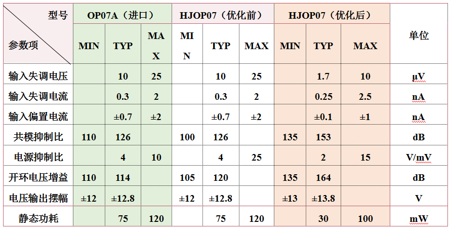
By comparing the electrical parameters of the three devices, it can be visually observed that the optimized HJOP07 has a smaller input offset voltage, higher common mode rejection ratio and power supply rejection ratio, greater open-loop voltage gain, and lower static power consumption. This indicates that the optimized HJOP07 has better electrical parameters.
Simulate experimental tests on the electrical parameters and drift characteristics (important electrical parameters) of the optimized device HJOP07. Under constant temperature conditions, a one month drift stability test was conducted on the optimized HJOP07 device. The test results showed that the drift error of the optimized device was approximately 0.8 μ V/mon, which fully met the parameter requirements of the imported device OP07A.
Based on the above experiments and comparative explanations, After optimization HJOP07, the electrical parameters continue to meet the requirements of previous devices, and the electrical parameters are better than those of previous devices. Imported devices can be updated and replaced as completed or old products
II.HJG620's improvement
G620is a low-power, high-precision instrumentation amplifier that can adjust the gain from1~10000. It features high precision, low nonlinearity error, low offset voltage, low bias current, low noise, short settling time, and small temperature drift. Due to its small size and low power consumption, it is very suitable for applications in high-precision data acquisition systems such as weighing equipment, sensor interfaces, multiplexing, as well as battery-powered, portable or mobile devices in various scenarios.
1. Packaging form
HJG620's packaging usesD08S2ceramic dual inline package and F08-06 ceramic flat package. Please refer to the appendix for specific packaging size drawings.
2. Lead out function
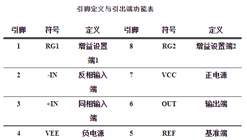
3. Comparison before and after optimization
Regarding the imported AD620, HJG620 before optimization and HJG620 after optimization, electrical parameter testing comparison was conducted., the electrical parameter test results are shown in the table below:
Comparison Table of Electrical Parameter Characteristics
Unless otherwise specified,VCC=+15V,VEE=-15V,RL=2kΩ,TA=+25℃。
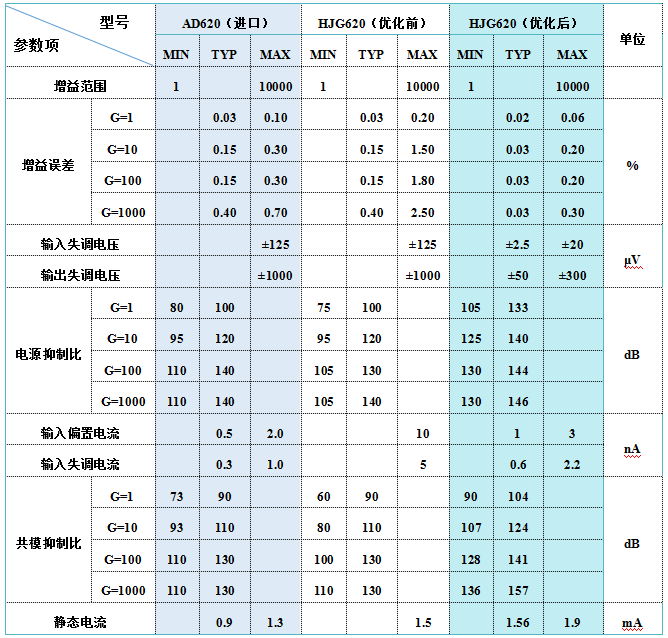
By comparing the electrical parameters of three types of devices, it can be intuitively found that the optimized device's electrical characteristic parameters are generally superior to those of previous products. Moreover, issues such as large gain error under high gain settings and poor common-mode voltage rejection under low gain settings present in previous products have been improved. Through comparative testing of electrical parameters, it was found that optimization performance is better and can update and replace old products.The electrical characteristic parameters of HJG620 are basically superior to previous products, and the problems of large device gain errors under high gain settings and poor common mode voltage suppression under low gain settings in previous products have been improved. By comparing the electrical parameter tests, it was found that the optimized HJG620's performance is better. It can be updated and replaced with old products.
AD620.'s design involves two input stages where both circuits were connected with a resistor of two input stages These two resistors enable the device to reliably withstand a maximum voltage of+15V400 Ω resistors, these two resistors enable the device to reliably and safely withstand up to+15V voltage or input overload for several hours at a current of 60mA; If the current does not exceed 6mA (IIN ≤ VIN/400 Ω), the anti input overload time will be longer. Due to the presence of this input resistor in series in the design, the instrument amplifier has sufficient capacity to withstand power on, power off, or when the input stage is affected by abnormal electrical surges. If there is no 400 Ω resistor, the device's function is easily damaged when there is an abnormal voltage in the input stage that momentarily exceeds the power supply voltage.
Considering the design concept of the imported AD620, the input stage of the instrument amplifier was also processed during the optimization and improvement of HJG620. A resistor of approximately 400 Ω was connected in series to the input stage of the device to enhance its ability to withstand abnormal surge signals, resulting in improved reliability of the optimized device.
Based on the above experiments and comparative explanations, After optimizationHJG620The electrical parameters continuously meet the requirements of previous devices, and the electrical parameters are better than those of previous devices.and imported devices, And it improves the reliability of the device, enabling updates and replacements for old products
In the next few years, it will be an important strategic opportunity period for the development of China's integrated circuit industry, as well as a critical period for the development of integrated circuits. While developing independent new products, the company will continuously complete the localization and replacement of existing components, and can focus on providing overall solutions. According to customers' special requirements, the company will research, improve, and optimize specialized integrated circuits and functional modules that can significantly enhance system performance, in order to meet customer needs to the greatest extent possible.
Hangjing Microelectronics will embrace the concept of "seeking development through innovation and survival through quality" and work together with everyone to tackle challenges and share opportunities! Realize high-level technological self-reliance and self-improvement.
3.Appendix
Key words:
improvementction,continuous
Next Page
Next page:
recommend News
Exploring the Advantages of Low Voltage Rail-to-Rail Operational Amplifiers: A Comprehensive Guide
Exploring the Advantages of Low Voltage Rail-to-Rail Operational Amplifiers In the fast-evolving field of electronics, the quest for devices that offer efficiency, precision, and versatility is unending. One such innovation that has made significant strides in this domain is the low voltage rail-to-rail operational amplifier (op-amp). These amplifiers have become increasingly popular due to their
2026-03-23
Understanding Precision Amplifiers for Data Acquisition Systems
Precision amplifiers play a critical role in data acquisition systems, which are essential for gathering and analyzing measurement data in various applications. These amplifiers are designed to enhance the accuracy and reliability of signals coming from different sensors and transducers, making them invaluable in fields such as industrial automation, medical devices, and environmental monitoring.
2026-03-22
Understanding the Role of Instrumentation Amplifiers in Bridge Sensor Applications
Understanding the Role of Instrumentation Amplifiers in Bridge Sensor Applications Table of Contents 1. Introduction to Instrumentation Amplifiers and Bridge Sensors 2. What Are Instrumentation Amplifiers? 3. Basics of Bridge Sensors: Types and Applications 4. Why Are Instrumentation Amplifiers Essential in Bridge Sensor Applications? 5. Key Design Principles of Instrumentation Amplifiers 6. Appl
2026-03-21
Optimizing Measurement Systems with Operational Amplifiers
Operational amplifiers (op-amps) are fundamental components in measurement systems, serving as versatile tools in various electronic applications. Their ability to amplify weak signals makes them indispensable in environments where precision is paramount. In this article, we will delve into the functionality of operational amplifiers, their applications in measurement systems, and the advantages t
2026-03-20
Unlocking the Potential: How Operational Amplifiers Enhance Analog Signal Conditioning
Unlocking the Potential: How Operational Amplifiers Enhance Analog Signal Conditioning Table of Contents 1. Understanding Operational Amplifiers 2. The Role of Analog Signal Conditioning 3. Key Features of Operational Amplifiers 3.1. High Input Impedance 3.2. Low Output Impedance 3.3. High Voltage Gain 4. Common Applications of Operational Amplifiers in Signal Conditioning 4.1. F
2026-03-19