
The analog characteristics and switching characteristics of electronic analog switches
Release time:
2021-07-28
Many engineers using analog switches for the first time often equate them entirely with mechanical switches. In fact, while analog switches have switching capabilities
Many engineers using analog switches for the first time often equate them completely with mechanical switches. In fact, although analog switches have switching capabilities, they differ from mechanical switches in that they also possess semiconductor characteristics.
The analog characteristics of analog switches
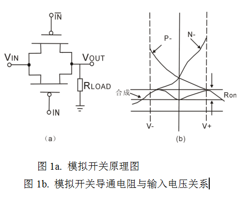
(1) The on-resistance (Ron) varies with the input signal (Vin)
Figure 1a is a simple schematic of an analog switch. From the figure, it can be seen that the normally open and normally closed channels of the analog switch are actually composed of two complementary N-channel MOSFETs and P-channel MOSFETs, allowing bidirectional signal transmission. If the on-resistances corresponding to different Vin values for the P-channel and N-channel MOSFETs are connected in parallel, Figure 1b shows how Ron varies with input voltage (Vin) under parallel structure. If temperature and power supply voltage effects are not considered, Ron shows a linear relationship with Vin, which leads to changes in insertion loss and causes total harmonic distortion (THD) in the analog switch. Additionally, Ron is also affected by power supply voltage, typically decreasing as power supply voltage increases.
(2) Analog switches have strict input signal ranges
Since analog switches are semiconductor devices, when the input signal is too low (below negative power supply voltage) or too high (above positive power supply voltage), the MOSFET is in reverse bias. When the voltage reaches a certain value (exceeding limits of 0.5 to 4V), the switch cannot operate normally; in severe cases, it may even be damaged. Therefore, when using analog switches, it is essential to ensure that input signals do not exceed specified ranges.
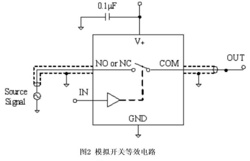
Some circuits of analog switches can be equivalent to Figure 2
(3) Charge injection
When using mechanical switches, we certainly hope for lower Ron because low resistance can reduce signal loss. However, for analog switches, low Ron is not suitable for all applications; lower Ron requires a larger chip area which results in higher input capacitance (parasitic capacitance). The charge variation caused by parasitic capacitance associated with NMOS and PMOS transistors is referred to as 'charge injection'. During each switching cycle, its charging and discharging processes consume more current and also generate positive and negative spikes. The time constant t=RC indicates that charging time depends on load resistance R and capacitance C, generally lasting several tens of ns. This indicates that lower Ron has longer turn-on and turn-off times. Therefore, selecting an analog switch should comprehensively weigh Ron against injected charge.
(4) Induced signals still leak out when switched off
This characteristic refers to when an analog switch transmits AC signals; even when switched off, some signals still pass through induction from the input side to the output side or from one channel to another channel. Generally speaking, as signal frequency increases, leakage becomes more severe.
(5) Transmission current is relatively small
Analog switches differ from mechanical ones; they typically only transmit small currents. Currently available CMOS technology-based analog switches allow continuous transmission currents mostly below 500mA.
(6) Logic control terminal drive current is extremely small
The drive current for logic control terminals of mechanical switches often reaches mA levels; sometimes it's difficult to drive them solely with digital I/O. In contrast, logic control terminals of analog switches have extremely small drive currents—generally below nA levels—allowing them to be directly driven by digital I/O to reduce power consumption and simplify circuits.
Switching characteristics of analog switches
(1) Signals can be transmitted bidirectionally
Some people habitually refer to both normally open and normally closed ends of an analog switch as input terminals while calling the common terminal an output terminal; however this is merely a temporary definition based on specific applications of the analog switch. Most analog switches allow bidirectional signal transmission; neglecting this point can easily lead to circuit issues such as reverse biasing voltages or backflow currents.
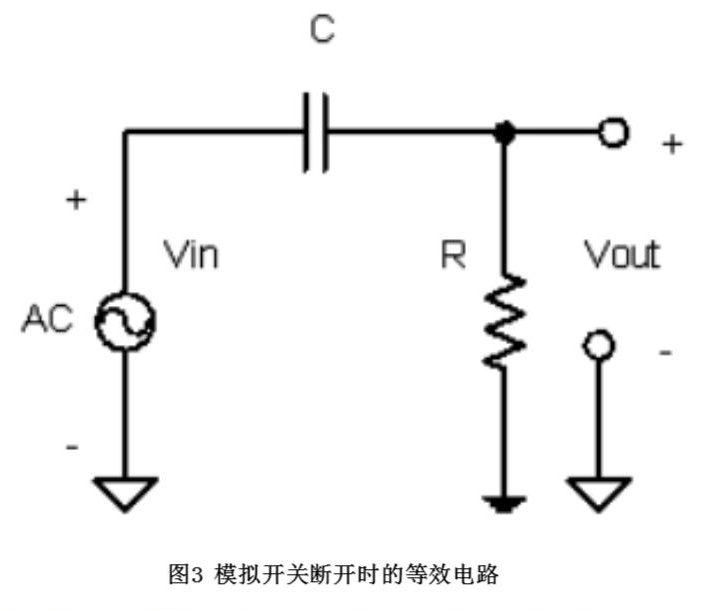
(2) Leakage current is extremely small when switched off
When an analog switch is off (OFF), it presents a high-resistance state with very little leakage current between its two transmission terminals—generally only below nA levels—with many having leakage currents around just about 1nA after being turned off. Such weak currents can be neglected in applications; at this point an analog switch can be considered ideally off.
The equivalent circuit of an analog switch when turned off is shown in Figure 3.
In summary, an analog switch is a semiconductor device with switching functionality that must fully utilize its switching capabilities while considering its semiconductor characteristics during application; otherwise unexpected troubles may arise.
Key words:
Previous Page
recommend News
Understanding High-Speed Amplifiers for Efficient Data Acquisition
High-speed amplifiers are essential in the field of data acquisition, particularly for applications that require rapid signal processing and high accuracy. These amplifiers are designed to boost weak electrical signals, making them more suitable for analysis and further processing. Key applications of high-speed amplifiers include scientific research, industrial automation, telecommunications, and
2026-07-02
Wideband Amplifiers: Bridging the Gap in Communication Technology
Wideband Amplifiers: Bridging the Gap in Communication Technology Table of Contents 1. Introduction to Wideband Amplifiers 2. What Are Wideband Amplifiers? 3. The Importance of Wideband Amplifiers in Communication Technology 4. How Do Wideband Amplifiers Work? 5. Applications of Wideband Amplifiers 6. Key Benefits of Using Wideband Amplifiers 7. The Future of Wideband Amplifiers in
2026-07-01
Essential Insights on Power Amplifiers for Motor Control Applications
Power amplifiers for motor control are vital components in various electronic systems, serving as the bridge between low-level control signals and the high-power requirements of motors. These amplifiers are designed to deliver significant power gains, enabling precise control over motor speed, torque, and direction. Understanding their functionality and selection criteria can greatly enhance the p
2026-06-30
Common Mistakes to Avoid When Using Rail-to-Rail Amplifiers
Common Mistakes to Avoid When Using Rail-to-Rail Amplifiers Rail-to-rail amplifiers are powerful tools in the electronics industry, enabling designers to maximize the output signal range of their circuits. While these amplifiers can significantly enhance performance, many users make common mistakes that can lead to suboptimal results. In this article, we will delve into these pitfalls, providing v
2026-06-29
Unlocking the Potential of Rail-to-Rail Amplifiers in Sensor Interfaces
Rail-to-rail amplifiers are pivotal components in modern electronic systems, particularly in sensor interfaces where precision and efficiency are paramount. These amplifiers are designed to operate over the full voltage range from the negative rail to the positive rail, enabling them to effectively utilize the entire supply voltage. This characteristic is especially beneficial in applications requ
2026-06-28