

Hangjing has launched a domestically produced high-voltage power operational amplifier.
Release Date:
2023-10-30
Source:
Technical Department/Marketing Department
Author:
Hangjing Microelectronics
Hangjing has launched a domestically produced high-voltage power operational amplifier.
In recent years, driven by the growing demand for domestic production in the integrated circuit industry, Hangjing Company has been committed to achieving full domestic sourcing across the entire IC supply chain. Following extensive market research, feasibility studies, and experimental validation, as well as leveraging its own technological expertise and ongoing R&D efforts, the company has now launched a fully domestically produced high‑voltage power operational amplifier designed and manufactured by Hangjing Microelectronics. HJGPA61 A , can fully replace imported components in situ PA61 and OPA541。
I. Overview
HJGPA61 A It is a product that complies with GJB2438 The high-voltage power operational amplifier for thick-film hybrid integrated circuits, as required by the standard, employs BeO The substrate screen-printing thick-film integration process not only effectively reduces the device’s thermal resistance but also enhances its reliability. By incorporating laser trimming, the devices can achieve even lower offset parameters.
HJGPA61A The device features low input offset voltage, low input offset current, a wide supply voltage range, and output… High peak current, etc. Its key feature is that the device’s package has no electrical connections, allowing for easy attachment of a heat sink. This device can drive resistive, capacitive, or inductive loads and is widely used in applications such as motor torque drives, cable actuators, and gyroscopic coil torque‑generating systems.
Table 1 HJGPA61A 、PA61、OPA541 Comparison Table
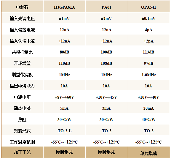
By comparison, it can be seen that, HJGPA61 A With imported components PA61、OPA541 The package is consistent, the lead‑out terminal functions are identical, and the electrical parameters are essentially the same.
Among them, comparison reveals that although OPA541 It offers the advantage of extremely low input offset parameters, but its typical quiescent current is 20mA , far exceeding the other two devices. When OPA541 When the device operates under high supply‑voltage conditions, its monolithic integrated design results in poor thermal dissipation, and the device itself exhibits substantial thermal power consumption, leading to severe self‑heating. HJGPA61A By employing a thick-film integrated design process, the device’s thermal resistance is not only significantly reduced but its reliability is also enhanced. HJGPA61A Compared to OPA541 It features lower thermal power consumption and superior heat dissipation, outperforming… OPA541。
Overall comparison: domestic aerospace-grade components HJGPA61 A Capable of fully replacing imported components. PA61 and OPA541。
II. Electrical Principle Block Diagram

Figure 1 HJGPA61A Principle block diagram
III. Package Type and Lead Terminal Functions
1 . Package type
Adopt TO-3-L Encased in a fully sealed metal housing, with external dimensions as shown in the figure below. 2 , See the product photos in the figure. 3。
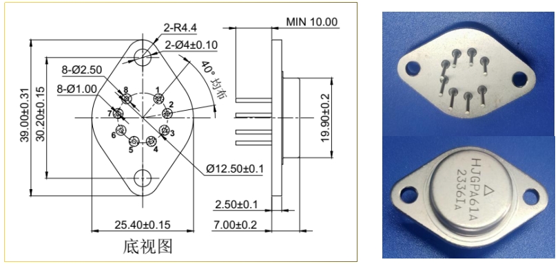
Figure 2: Dimensional drawing of the TO-3-L all-metal hermetic package Figure 3: Actual photograph of the HJGPA61A product
2 . Lead-out terminal function
Table 2 Package Pin Function Table
Pin |
Symbol |
Functionality |
Pin |
Symbol |
Functionality |
1 |
OUT |
Output |
8 |
CL- |
Current-limiting resistor |
2 |
CL+ |
Current-limiting resistor |
7 |
NC |
Empty foot |
3 |
+VS |
Positive power supply |
6 |
-VS |
Negative power supply |
4 |
+IN |
Non-inverting input |
5 |
-IN |
Inverting input |
IV. Electrical Characteristics
Unless otherwise specified, V CC = +45V , V EE = -45V, T A = +25℃ 。
Table 3 Electrical Characteristics Table
Parameter Name |
Test conditions |
Standard value |
Unit |
||
Minimum value |
Typical value |
Maximum value |
|||
Input offset voltage |
|
|
±1 |
± 6 |
mV |
Input Offset Voltage Temperature Drift * |
-55℃~+125℃ |
|
±10 |
±100 |
uV/°C |
Input bias current |
|
|
12 |
30 |
nA |
Input bias current temperature drift * |
-55℃~+125℃ |
|
±50 |
±500 |
pA/°C |
Input Offset Current |
|
|
±12 |
±30 |
nA |
Input Offset Current Temperature Drift * |
-55℃~+125℃ |
|
±100 |
|
pA/°C |
Input resistance * |
|
|
100 |
|
MΩ |
Common-mode input voltage range * |
|
±V S -10 |
±V S -5 |
|
V |
Common-mode rejection ratio |
|
64 |
80 |
|
dB |
Open-loop gain |
|
96 |
110 |
|
dB |
Gain-bandwidth product |
|
|
1 |
|
M Hertz |
Power bandwidth |
I O =2A , V O =60V PP |
5 |
15 |
|
kilohertz |
Output voltage |
I O =5A |
±V S -10 |
±V S -5 |
|
V |
I O =2A |
±V S -7 |
±V S -4 |
|
||
I O =35 mA |
±V S -6 |
|
|
||
Continuous output current |
|
± 8 |
|
|
A |
Quiescent current |
|
|
5 |
12 |
mA |
Note: With * The parameter is the design guarantee.
V. Typical Applications
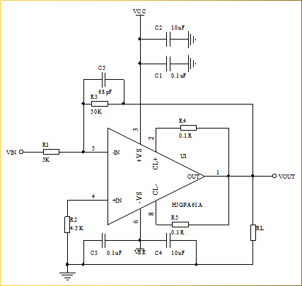
HJGPA61 Typical Application Diagram
1.R4 and R5 It refers to the output sourcing current of an operational amplifier ( Source ) and injection current ( Sink ) current‑limiting protection resistor; when the output current exceeds the set threshold, the current‑limiting resistor activates the protection circuit to prevent output‑stage short circuits that could lead to device failure.
2. When operating in high‑power output conditions, an appropriate heat sink must be added to prevent heat from accumulating and damaging the device.
VI. Relevant Products and Domestic Substitution Status
Table 4 Product substitute
Serial number |
Product Name |
Imported model |
Aviation crystal model |
Alternative form |
1 |
Power operational amplifier |
LH0021 |
HJ0021 |
In-situ substitution |
2 |
Power operational amplifier |
LH0041 |
HJ0041 |
In-situ substitution |
3 |
Buffer |
LH0002 |
HJ0002 |
In-situ substitution |
4 |
High-Voltage Power Operational Amplifier |
PA83 |
HJPA83 |
In-situ substitution |
5 |
High-Temperature, High-Current Operational Amplifier |
OPA544 |
HJ544C |
In-situ substitution |
6 |
Dual-channel power amplifier |
OPA2544 |
HJ2544C |
Functional substitution |
Keywords:
Hot News
Leave a Message Online
*Note: Please ensure that all information provided is accurate and keep your contact details up to date. We will get in touch with you as soon as possible.
Request for Samples / Product Manuals / Contact Information:
Mr. Jia:13022932841(WeChat)
Landline:029-89259995Transfer 833
Technical Support / Contact Information:
Mr. Zhao:13572473285
Landline:029-89259995Transfer to 803
Ms. Xu:18729396827
Company landline:029-89259995
Fax: 029-89259996
Unit 4, Building 6, Beihang Science and Technology Park, Hangtian Middle Road, Aerospace Base, Chang’an District, Xi’an, Shaanxi Province
