

A Further Discussion on High-End Switches
Release Date:
2022-02-16
Source:
Author:
Hangjing Microelectronics
In control systems, it is often necessary to distribute power to one or more payloads at specific moments. This requires the installation of switches at the downstream end of the power busbar. There are two common switch modes, as shown in the figure below:
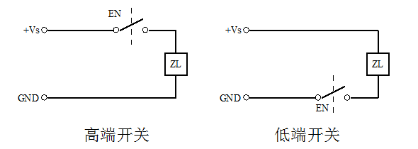
Both types have their applications. High-end switches are primarily used in high- and medium-voltage environments, while low-end switches are mainly employed in 5V and 3.3V applications.
High-end switch
Below, we will primarily analyze high-end switches.
In principle, relays are the most convenient solution for high‑end switching applications, and they exhibit very low contact resistance—typically on the order of a few milliohms, depending on the contact‑area size. However, modern electronic systems generally seek to minimize the use of relays. The reason is that during the relay’s make or break transitions—when the gap between contacts is on the order of micrometers—arcing can easily occur, particularly in medium‑ and high‑voltage applications, thereby compromising the system’s operational life.
Therefore, in modern electronic systems, MOSFETs are typically used as switching elements, often referred to as “contactless switches.” Compared with relays, they have higher conduction losses (since the on‑state resistance of a MOSFET cannot be made extremely low), but their key advantage is the absence of mechanical movement, resulting in a longer service life. Additionally, they enable fast switching, which is critical for certain types of loads. When using MOSFETs as high-side switches, there are two distinct scenarios:
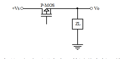
P‑MOS: Easy to implement. However, due to the low mobility of “holes,” it is generally suitable only for medium‑voltage (10 V to 100 V) and medium‑power (≤10 A) applications.
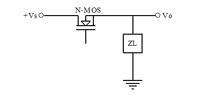
N‑MOS: Requires a “floating gate” drive, which is difficult to implement. However, due to the high mobility of electrons, it is well suited for high‑voltage (≥200 V) and high‑power (≥50 A) applications.
Both types of switches can arbitrarily adjust the on/off speed to suit different Z conditions. L Load requirements. In the figure, ΔV represents the MOSFET’s on‑state voltage drop.
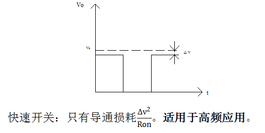
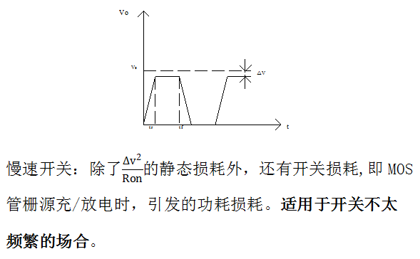
Due to conduction losses and switching losses, the control strategy for the MOSFET must be adjusted in practical applications based on system control requirements and load conditions, and appropriate thermal management must be implemented for the device.
Implementation methods for high-end switches
So, what components should a fully functional high‑end switch comprise? Below, we’ll use a P‑MOS transistor as an example to illustrate this. (See the block diagram below.)
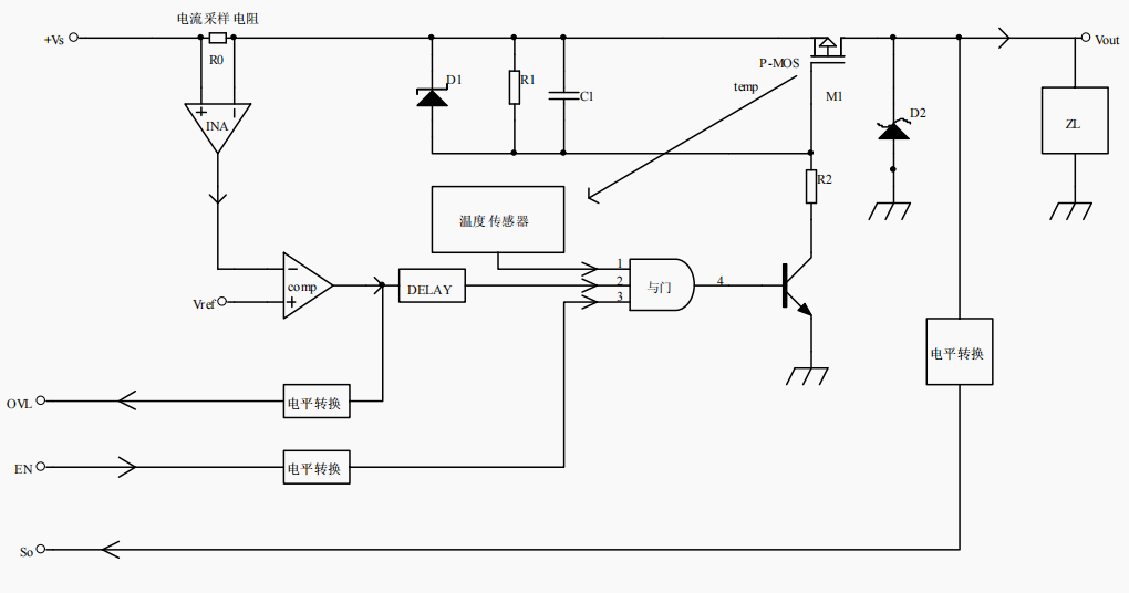
As can be seen from the block diagram above, a typical medium-voltage, medium-power high-end switch consists of a switching transistor (M 1 ), current sampling (R o ), a high common-mode voltage instrumentation amplifier (INA), a comparator (COMP), delay circuits, temperature sensors, logic gates, level‑shifting circuits, and RC networks for controlling the turn‑on/turn‑off slew rate, among other components. “OVL” indicates overcurrent, “So” indicates output status, and “EN” serves as the enable/control signal. This configuration is particularly well suited for 28‑V aircraft power systems, as it features a simple architecture, compact size, and ease of implementation.
The following are several key points of this system that require special clarification:
l Power consumption. It mainly depends on M. 1 The on-resistance R on (under the assumption of negligible switching losses) and the value of the current-sensing resistor Ro. In general, Ron and R are selected… o As small as possible.
l Switching rate control. By adjusting R 1 , R 2 , C 1 Completion depends on the characteristics of the load. If the load exhibits purely resistive behavior, it is suitable for fast switching control, thereby reducing M. 1 Dynamic power consumption. If the load is capacitive or inductive, only a slow-switching control strategy can be employed. This is because the voltage across a capacitor and the current through an inductor cannot change instantaneously. If the switching rate is too fast, it can easily trigger false overcurrent detections and may also introduce noise into the power supply system.
l Overcurrent hiccup mode, achieved by adjusting the comparison between output delay and control M 1 The rise/fall times are jointly determined. The hiccup mode is a feature that all power supply systems should possess, exhibiting the characteristics shown in the figure below.
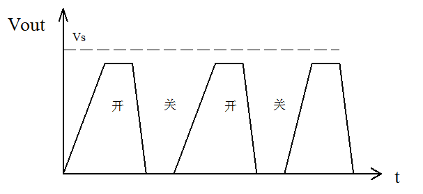
In other words, when the upstream device sends an EN signal, the high‑end switch should be in its normal powered‑on state. However, due to the load Z… L If an overload occurs (such as a short circuit), the current-sensing resistor R… 0 This overcurrent is detected, and the local controller then controls M. 1 Deadline. M 1 After the cutoff, the overcurrent condition disappears, and normal power supply is restored. However, since the overcurrent state persists, the system attempts to turn off M again. 1 . In this cyclical manner, a waveform similar to that shown in the figure above emerges, commonly referred to as “hiccup mode.”
Its importance is reflected in two aspects: first, by means of the local on-off switching transistor M. 1 To protect the tube from burning out. Second, after the host computer detects that the overcurrent indication signal “OVL” has tripped a specified number of times, it issues an EN command to remotely shut down M. 1。
l Level translation is primarily implemented to ensure signal-level compatibility with the host central control computer. Sometimes, due to the central control computer and +V… S If the power supply system is not grounded, isolation must also be implemented.
l D 1 Its function is to protect M. 1 The gate-source does not break down. D 2 The role of M is 1 It provides load freewheeling when disconnected.
The foregoing discusses the implementation approaches for high-end medium-voltage, medium-power switches.
Implementation Strategies for High-Voltage, High-Power, High-End Switches
Below is a brief overview of the implementation strategy for a high-voltage, high-power, high-end switch.
The primary design consideration for high‑voltage, high‑power, high‑end switches is to minimize power loss. Consequently, the “shunt”‑type current sensing approach described earlier is no longer suitable. Furthermore, due to mobility limitations of P‑MOS transistors and manufacturing‑process constraints, it is challenging to achieve both a breakdown voltage exceeding 200 V and a low on‑state resistance RDS(on). o n First, it must be implemented using N‑MOS transistors. Second, since crosstalk on the power ground (PGND) can interfere with or even damage the host central control computer, the OVL, EN, and SO signals must be isolated. Finally, heat dissipation is a concern; in some cases, air cooling is no longer sufficient, necessitating oil‑cooling or water‑cooling for the M. 1 Heat dissipation. (See the block diagram below.)
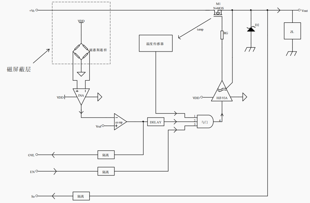
As shown in the figure above, an N‑MOSFET is used as the switching element, a magnetic Wheatstone bridge serves as the current-sensing circuit, and the HJ393A driver is employed to drive the N‑MOSFET. A temperature sensor is incorporated to measure the N‑MOSFET’s junction temperature, and a control supply voltage V must be introduced. DD Such a configuration helps reduce power consumption (without the aforementioned R). o ), it can not only drive the floating gate of an N-MOS transistor but also provide over-temperature protection.
As a well‑designed high‑end switch, in addition to its basic components, it must also account for the characteristics of the load (i.e., ZL in the figure above). Purely resistive loads do not exist; in practice, most loads are combinations of resistance R, capacitance C, and inductance L. The energy‑storage effect of the capacitor can cause the switching transistor M… 1 The inductor’s freewheeling action during the instant of turn-on will cause M. 1 During turn-off, it must withstand negative voltage pulses; all these factors will affect the power transistor M. 1 It has a negative impact on long-term reliable operation.
Finally, as a high-end switch designed for harsh environments, its ability to withstand environmental stresses—such as thermal stress, shock and vibration, and electromagnetic interference—should also be taken into account.
Keywords:
Hot News
Leave a Message Online
*Note: Please ensure that all information provided is accurate and keep your contact details up to date. We will get in touch with you as soon as possible.
Request for Samples / Product Manuals / Contact Information:
Mr. Jia:13022932841(WeChat)
Landline:029-89259995Transfer 833
Technical Support / Contact Information:
Mr. Zhao:13572473285
Landline:029-89259995Transfer to 803
Ms. Xu:18729396827
Company landline:029-89259995
Fax: 029-89259996
Unit 4, Building 6, Beihang Science and Technology Park, Hangtian Middle Road, Aerospace Base, Chang’an District, Xi’an, Shaanxi Province
