An overview,
The circuit is a thick film hybrid integrated circuit composed of OP37A chip and protection element,and the main electrical parameter is better than that of single OP37A.Characterized by disturbance voltage of 10 mu V,offset voltage temperature coefficient of 0.2 mu V/℃,long-term stability of 0.2 mu,V/month without compensation components and require no external antistatic protection components.
Mainly used in electronic systems,preamplifier,error amplifier,dc signal amplification,direct coupling amplifier,instrumentation amplifier,two-way matching amplification requirements such as high precision,low drift,high reliable and signal processing occasions such as antistatic.It is especially suitable for the miniaturized high performance instruments in defence,military and industrial fields.
The device has excellent antistatic ability,and the threshold voltage of electrostatic damage is more than 4000V(the voltage of static damage threshold of normal OP37 is about 700~1000V).
The surge performance of the device is significantly enhanced.
There are lower input offset voltages,typical values of about several mu V,generally do not need external zero;
Low drift(0.2 u V/℃),the conversion rate of 17 V/u(s),the gain bandwidth(63 MHZ),low noise(NVP 80-p);
In addition to increasing integration,two(four)operational amplifiers have good consistency.
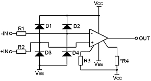
Electrical schematic diagram
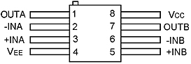
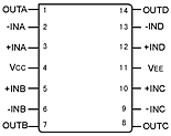
3.Package form and outlet function.
1.DOP-37AMJ is packaged with f08-04a ceramic flat shell,and the dimensions are shown in FIG.9.
(top view)
2. Qop-37amj is encapsulated with mp-14b double-column metal sealed package, and the dimensions are shown in figure 11.
(top view)
Iv.Absolute maximum rating.
Short circuit duration of power supply voltage plus or minus 22V output.
Input voltage of plus or minus 22 v work-55~+175℃temperature range
Dissipation power of 600 mw(F08-04 A)lead soldering temperature(10 s)+300℃
800 mw(MP-14 b)
V.electrical characteristics
Unless otherwise stated,VCC=+15V,VEE=-15V,-55℃≤TA≤+125℃。
|
parameter
|
symbol
|
The test conditions
|
Specification values
|
unit
|
|
The minimum
|
A typical
|
The biggest
|
|
Input offset voltage
|
VIO
|
TA=+25℃
|
|
10
|
25
|
μV
|
|
|
|
30
|
100
|
|
Input offset voltage temperature drift coefficient
|
αVIO
|
|
|
0.2
|
1.0
|
μV/℃
|
|
Long time stability of offset voltage*
|
VIO/T
|
TA=+25℃
|
|
0.2
|
1.0
|
μV/mo
|
|
Input offset current
|
IIO
|
TA=+25℃
|
|
7
|
35
|
nA
|
|
|
|
15
|
100
|
|
Input bias current
|
IIB
|
TA=+25℃
|
|
±10
|
±80
|
nA
|
|
|
|
±30
|
±100
|
|
Input noise voltage density*
|
en
|
TA=+25℃
fO=10Hz
fO=100Hz
fO=1000Hz
|
|
3.5
3.1
3.0
|
5.5
4.5
3.8
|
nV/
|
|
Input noise voltage*
|
enp-p
|
TA=+25℃,0.1~10Hz
|
|
0.08
|
0.18
|
μVp-p
|
|
Input noise current density*
|
In
|
TA=+25℃
fO=10Hz
fO=100Hz
fO=1000Hz
|
|
1.7
1.0
0.4
|
4
2.3
0.6
|
pA/
|
|
Differential input resistance**
|
RIN
|
TA=+25℃
|
1.5
|
6
|
|
MΩ
|
|
Common mode input resistance**
|
RINCM
|
TA=+25℃
|
|
3
|
|
GΩ
|
|
Input voltage range**
|
VIR
|
TA=+25℃
|
±11
|
±12.3
|
|
V
|
|
Common mode rejection ratio
|
CMRR
|
TA=+25℃,VCM=±11V
|
114
|
126
|
|
dB
|
|
Power supply voltage rejection ratio
|
PSRR
|
TA=+25℃,VS=±4~±18V
|
100
|
120
|
|
dB
|
|
Open loop voltage gain
|
AVD
|
RL≥2kΩ
|
TA=+25℃
|
120
|
125
|
|
dB
|
|
|
110
|
120
|
|
|
Maximum output voltage range
|
Vopp
|
RL=2kΩ
|
±11.5
|
±13.5
|
|
V
|
|
RL=600Ω , TA=+25℃
|
±10
|
±11.5
|
|
|
Conversion rate**
|
SR
|
TA=+25℃,RL≥2kΩ
|
11
|
17
|
|
V/μs
|
|
Gain bandwidth product**
|
GBW
|
TA=+25℃, fO=10kHz
|
45
|
63
|
|
MHz
|
|
Open loop output resistance*
|
RO
|
TA=+25℃,VO=0,IO=0
|
|
70
|
|
Ω
|
|
Static power consumption (single-channel operational amplifier)
|
PD
|
TA=+25℃,VO=0V
|
|
90
|
140
|
mW
|
|
Threshold voltage of antistatic damage*
|
ESD
|
The human body model
|
4.0
|
5.5
|
|
kV
|
|
* sample test ** design guarantee


